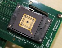
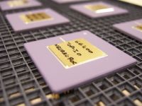
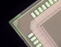
Chip Gallery
Making chips at µSystems, Newcastle University
The µSystems group, in support of its scientific and technological research, regularly design chips for fabrication and test the results to enhance our technological investigations. To this end, we have been engaged in establishing a first-class chip testing facility in the µSystems lab. To date, most projects related to hardware circuit and systems design have produced chip designs and the majority of these have been studied through testing of fabricated chips. A collection of some of our recent chips are listed on this page below.
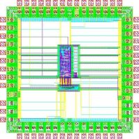
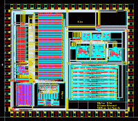
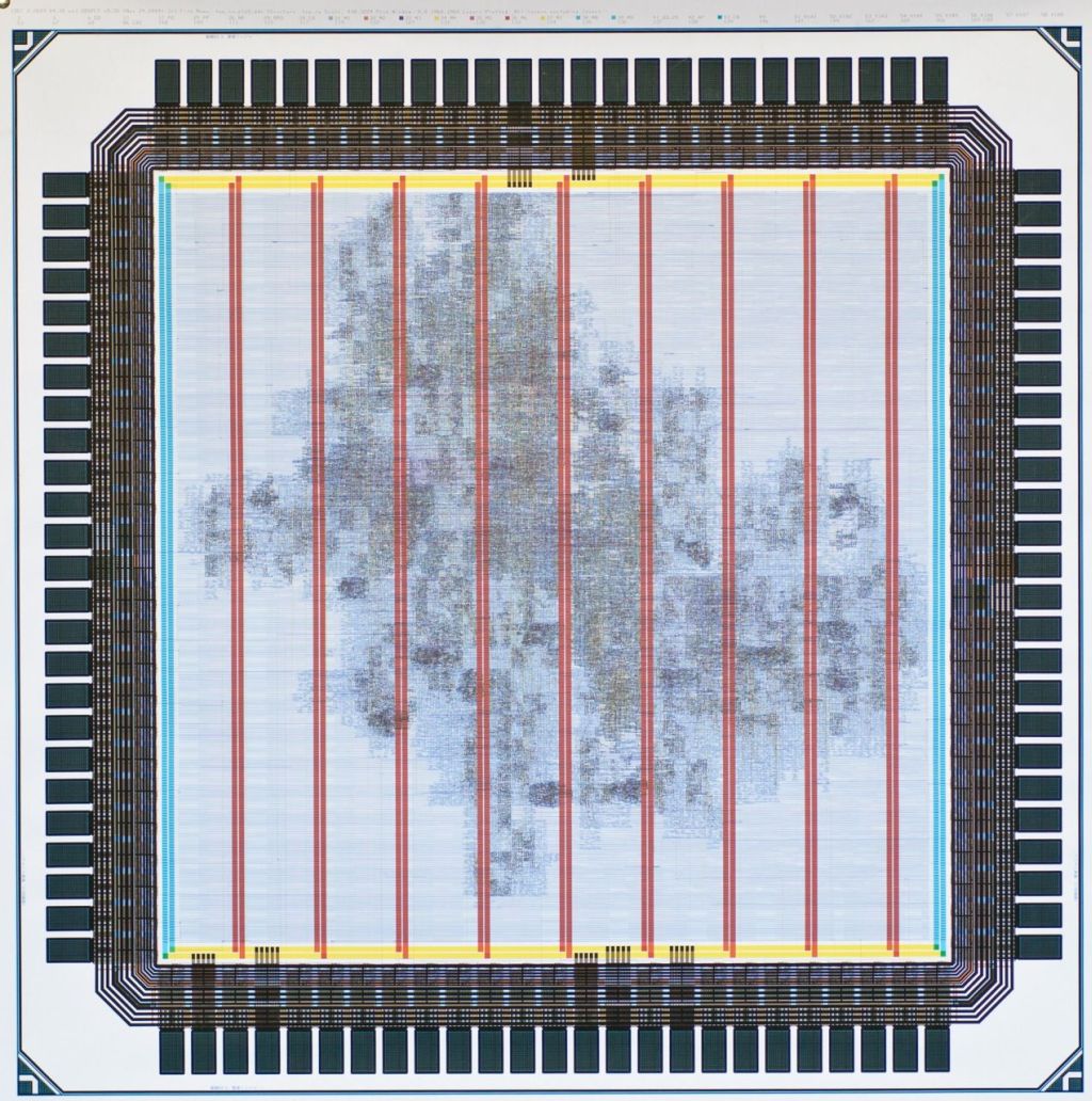
Reconfigurable Asynchronous Intel 8051 Microprocessor
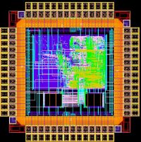
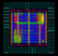
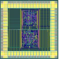
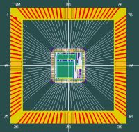
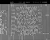
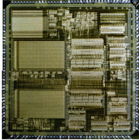
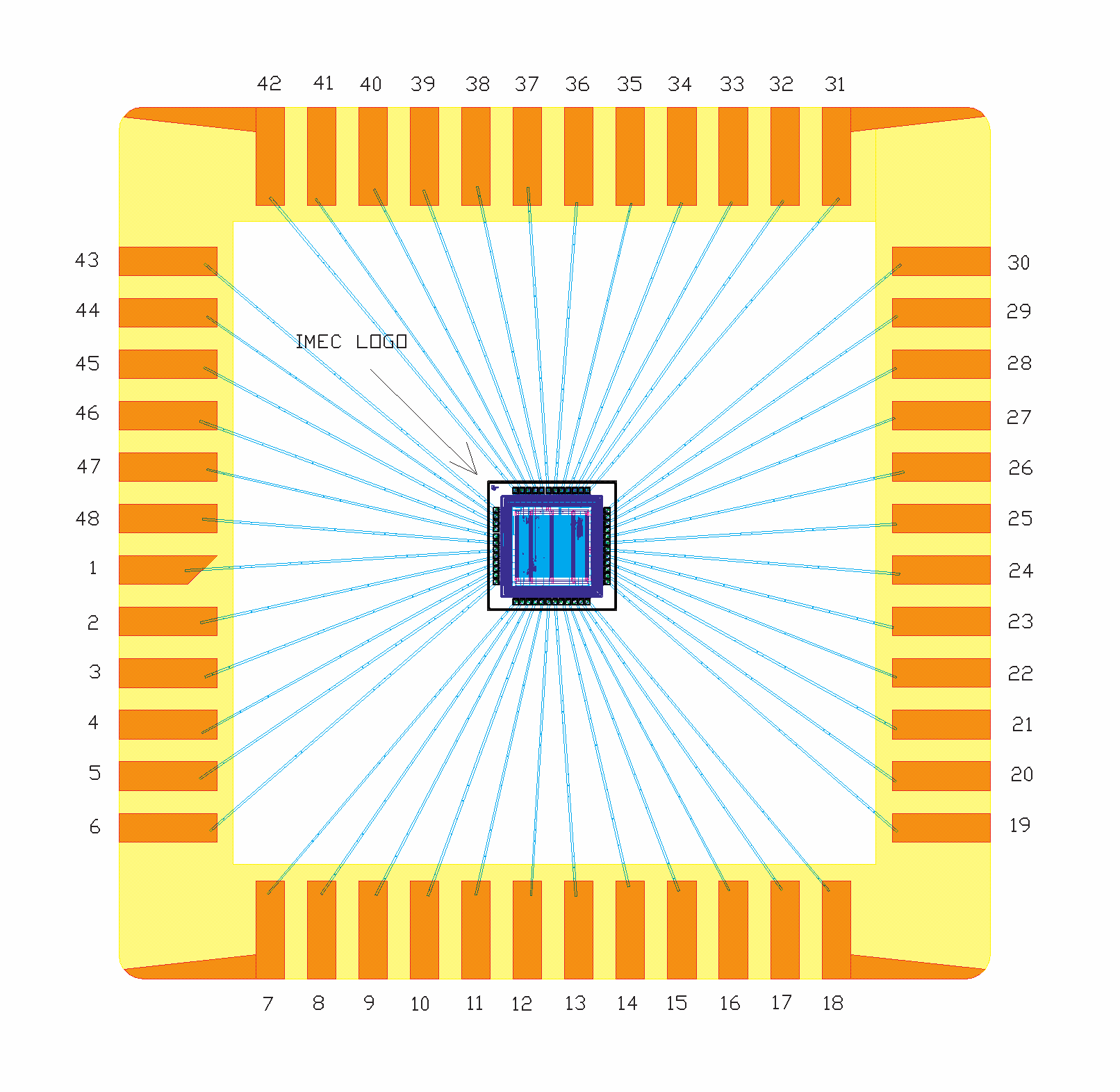
This demonstration chip contains a reconfigurable Asynchronous Intel 8051 Microprocessor. The main core of about 17,000 cells and two RAM blocks occupy 3mm2 of silicon area. The original (Intel 8051) instruction set (255 instructions) was implemented in the control logic based on the Conditional Partial Order Graph approach. The self-timed data path is based on the bundled-data approach with adjustable matching delay lines to achieve robust operation under a wide range of supply voltages and various operating conditions. The data path was also extended with an extra set of arithmetic units: one optimised for energy consumption and another optimised for performance, which enables multi-modal functionality and fault tolerance.
Year: 2013
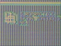
Technology: STMicroelectronics 130nm through CMP (Circuits Multi-Projects ) service
Contact: Maxim Rykunov, maxim.rykunov@ncl.ac.uk
Relevant papers:
M. Rykunov, A. Mokhov, D. Sokolov, A. Yakovlev and A. Koelmans, Design-for-Adaptivity of Microarchitectures, Proceedings of the 24th IEEE International Conference on Application-specific Systems, Architectures and Processors, Washington D.C., USA, June 2013.
A. Mokhov, M. Rykunov, A. Iliasov, D. Sokolov, A. Yakovlev and A. Romanovsky, Synthesis of processor instruction sets from high-level ISA specifications, in IEEE Transactions on Computers, 2013.
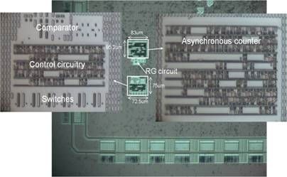
Reference-free voltage sensor
The voltage sensor was fabricated in the UMC 180nm CMOS process. The area occupied by the sensor circuitry is 0.013 mm2. The chip contains an asynchronous counter, the internal reference generator circuit, the self-timed dynamic comparator and the control unit. The aim for this fabrication is to prove the feasibility of voltage sensing through proposed charge-to-digital technique using a fully internalized reference. The chip was tested successfully through performing measurements over the voltage range from 1.8V down to 0.8V.
Year: 2012
Contact: Reza Ramezani, reza.ramezani@ncl.ac.uk
Relevant papers:
R. Ramezani, A. Yakovlev, F. Xia, J. Murphy and D. Shang, Voltage Sensing Using an Asynchronous Charge-to-Digital Converter for Energy-Autonomous Environments, IEEE Journal of Emerging and Selected Topics in Circuits and Systems (JETCAS), vol.3, No. 1, pp. 35-44, 2013.
Patent:
Apparatus and method for voltage sensing, A Yakovlev, R. Ramezani and T. Mak, Newcastle University, GB Patent Number 2479156, 30 March 2010.

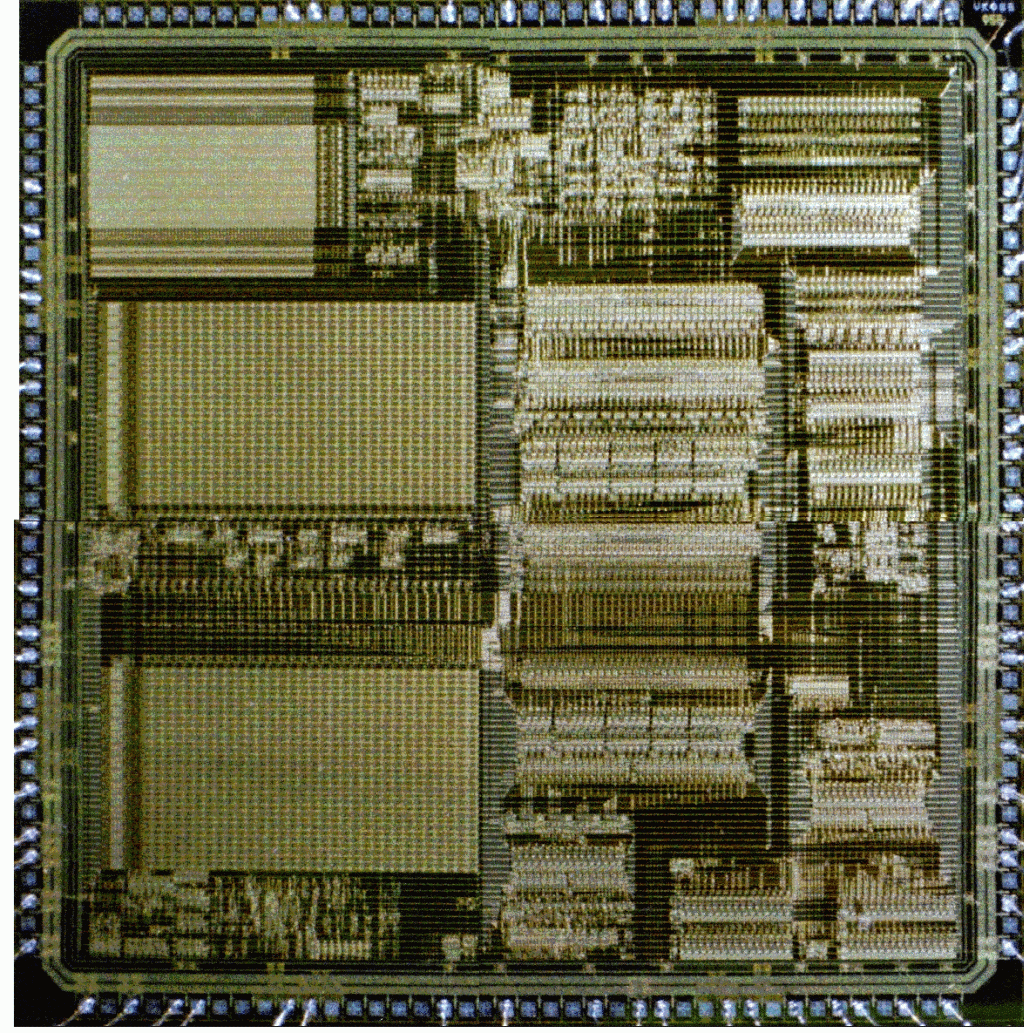
ASRAM
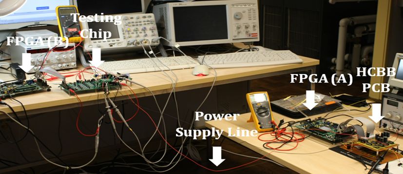
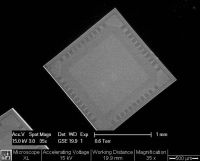
The world's first fully asynchronous (self-timed) SRAM chip was made in 90nm CMOS technology to demonstrate the group's ASRAM design method. This chip contains 64k bit of SRAM under full speed-independent (SI) control for self-timed operations. Part of the Holistic Energy Harvesting project this chip has been demonstrated to work under unstable and non-deterministically variable Vdd across a range of 1.2 to 0.7 volts and retain data down to 0.4 volts in a natural sleep mode. When Vdd is raised again the memory will wake up from where it halted with all states and data intact and resume normal operation. Testing circuits are also included on-chip, with the chip itself having dual power supply lines able to have the memory working under externally controlled variable Vdd and testing circuits working under stable nominal Vdd.
Year: 2011
Technology: UMC 90nm through Europractice
Project: Holistic Energy Harvesting
Contact: Dr Delong Shang, delong.shang@ncl.ac.uk
Relevant papers:
Baz A, Shang D, Xia F, Yakovlev A. Self-timed SRAM for Energy Harvesting Systems. Journal of Low Power Electronics 2011, 7(2), 274-284.
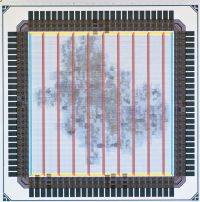
Neural-NOC
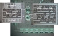
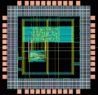
A demonstration chip in 90nm CMOS containing a reconfigurable neural network structure with hybrid interconnect. Consisting of 15 configurable blocks for neural network simulation connected by a configurable interconnect, the chip measures 1.8x1.8mm, contains over 180 thousand cells and took the best part of 4 months of work to implement. Each block contains one neuron model and ten synapses with learning capability. To complement the local routing resource, a single Network-on-Chip tile is superimposed; packets can be routed on and off chip for testing and demonstration. The chip is intended as a demonstration of a concept for a hardware neural network simulation platform for biological neural network models - which are massively parallel but have mostly local connectivity - for which a hybrid communication structure should provide adequate local resources that can scale as the network simulation grows larger.
Year: 2010
Technology: TSMC 90nm through Europractice mini@sic service
Project:
Contact: Robin Emery, r.a.emery@ncl.ac.uk
Relevant papers:
R. Emery, A. Yakovlev and G. Chester, Connection-Centric Network for Spiking Neural Networks, Proceedings of the 3rd ACM/IEEE International Symposium on Networks-on-Chip (NoCs 2009), San Diego, CA, USA, May 2009, IEEE, pp. 144-152.
Script 1 & 2
The chip designs implemented two co-processors with a AMBA-APB interface, a AES-128 encrypter (SCRIPT1) and 64-bit Floating Point Unit (SCRIPT2), and proved to be working correctly. They implemented the research conducted and by products of SCRIPT, EPSRC's Follow-on-Fund commercialization fund, where we came first against 113 other red-brick universities in 2008 in collaboration with Renesas Labs, Japan and raising 135k.
The chips were a proof-of-concept silicon to support two new patent disclosures to Newcastle's Business Development Directorate Unit.
Year: 2010
TSMC 90nm through Europractice mini@sic service
Projects: SURE and SCRIPT (funded by EPSRC)
Contact: Julian Murphy, j.p.murphy@ncl.ac.uk
SYRINGE2 Time-to-Digital Converter and Neuron Chip.
A High Resolution Flash Time-to-Digital Converter (TDC) was developed on a 130nm chip to investigate timing faults caused by the violation of internal timing parameters, such as clock jitter, clock skew and set-up and hold times. The TDC offers the possibility of measuring these timing parameters on-chip to the order of a single picosecond. The chip also contains demonstration circuits of a Leaky Integrate-and-Fire Neuron and an Asynchronous Pulse Generator for use in a biologically inspired reconfigurable neural network.
Investigation into the cause of timing problems cannot satisfactorily be undertaken by external equipment, due to the remoteness of external equipment from the source of the problem. Therefore, on-chip measurement circuits such as Time-to-Digital Converters (TDCs) are ideal for measuring accurately the relationship between two or more physical events to establish whether they operate according to specifications. In addition the method has the effect of reducing the measurement errors introduced by process, temperature and voltage variation, by implementing a statistical technique which relies on counting the number of high outputs.
Year: 2008
Technology: UMC 0.13um through Europractice
Project: SYRINGE (EPSRC Grant EP/C007298/1)
Contacts: Nikolaos Minas - Nikolaos.Minas@ncl.ac.uk, Robin Emery - r.a.emery@ncl.ac.uk


SURE Galois Encoded Logic AES-128 IP core Proof of Concept Chip. Implements side-channel secure "high radix" AES-128 encryption in a fully parallel architecture to investigate the security and study the market feasibility of the technology.
Year: 2008
Technology: UMC 0.13um through Europractice
Projects: SURE (EPSRC Grant EP/F016786/1)
NEGUS1 Phase-Encoding Demonstrator Chip. Contains different "flavours" of phase-encoding signalling to evaluate feasibility and performance of the scheme.
Year: 2007
Technology: UMC 0.13um through Europractice
Projects: NEGUS (EPSRC Grant EP/C512812/1)
Relevant papers:
D'Alessandro, C. (2007), Fast point-to-point serial link using Phase-Encoding, in 'Proceedings of the 3rd UK Embedded Forum'.
D'Alessandro, C.; Bystrov, A. & Yakovlev, A. (2007), 'Improved phase-encoding signalling', Electronics Letters 43(4), 216--217.
D'Alessandro, C.; Mokhov, A.; Bystrov, A. & Yakovlev, A. (2007), Delay/Phase Regeneration Circuits, in 'Proceedings. 13th International Symposium on Asynchronous Circuits and Systems. ASYNC 2007'.
D'Alessandro, C.; Shang, D.; Bystrov, A. & Yakovlev, A. (2005), PSK Signalling on SoC Buses, in 'Integrated Circuit and System Design. Power and Timing Modeling, Optimization and Simulation. Proceedings of PATMOS 2005', Springer.
D'Alessandro, C.; Shang, D.; Bystrov, A.; Yakovlev, A. & Maevsky, O. (2006), Multiple-Rail Phase-Encoding for NoC, in 'Asynchronous Circuits and Systems, 2006. 12th IEEE International Symposium on', pp. 107--116.
SYRINGE1 chip contains a robust synchroniser which maintains the value of its metastability time constant in the event of large Vdd variations (with dynamic current control during metastability). The chip also contains an on-chip measurement circuit which extends the measurement of synchronizers into the deep metastability region.
Year: 2006
Technology: CMOS UMC 0.18um fabricated by Europractice
Projects: SYRINGE (funded by EPSRC)
Relevant papers:
J. Zhou, D.J. Kinniment, G. Russell and A. Yakovlev, A Robust Synchronizer Circuit, Proceedings of the IEEE Computer Society Annual Symposium on VLSI (ISVLSI'06), Karlsruhe, Germany, March 2006, pp. 442-443.
J. Zhou, D.J. Kinniment, G. Russell, and A. Yakovlev, On-Chip Measurement of Deep Metastability in Synchronizers, IEEE Journal of Solid-State Circuits, Vol. 43, No. 2, 2008.
SCREEN2 Chip contains different (synchronous single-rail and power-balanced) versions of AES S-box.
Year: 2006
Technology: CMOS AMS 0.18um fabricated by Europractice
Projects: SCREEN (funded by EPSRC)
Relevant papers:
J. Murphy, A. Yakovlev, Power-balanced Asynchronous Logic, Proc. 17th European Conference on Circuit Theory and Design (ECCTD), 29 August - 2 September 2005.
J. Murphy, A. Bystrov and A.Yakovlev, Self-Checking Circuits for Security Applications, 11th Annual International Mixed-Signals Testing Workshop (IMSTW’05), Cannes, France, June 2005, pp. 278-285.
SCREEN1 Chip contains AES encryption core design using alternating spacer dual-rail signalling for power balancing (generated from synchronous RTL using in-house tool VeriMap).
Year: 2005
Technology: CMOS AMS 0.35um fabricated by Europractice
Projects: SCREEN (funded by EPSRC)
Relevant papers:
J. Murphy and A. Yakovlev. An Alternating Spacer AES Crypto-Processor, Proc. of ESSCIR 2006, Montreux, Switzerland, Sept. 2006, pp. 126-129.
D. Sokolov, J. Murphy, A. Bystrov and A.Yakovlev, "Design and Analysis of Dual-Rail Circuits for Security Applications", IEEE Transactions on Computers, Vol. 54, No.4, pp. 449-460, April 2005.
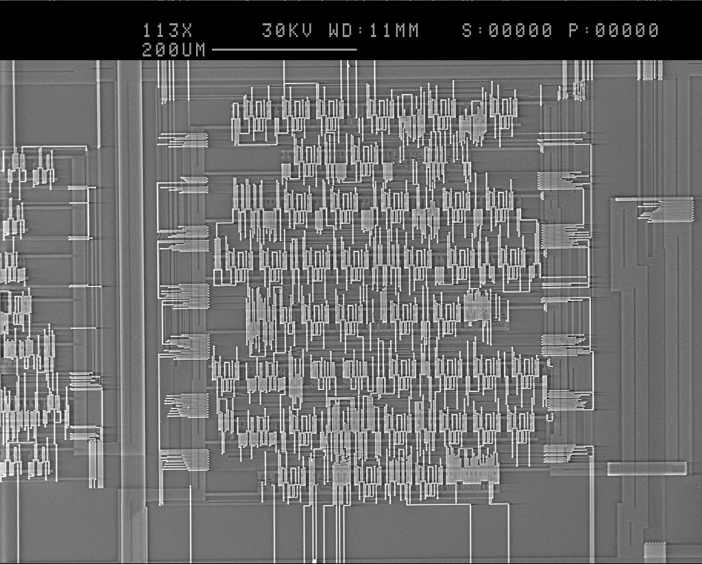
TMC Chip contains a time-measurement circuit, including time amplifier and time-to-digital converter.
Year: 2003
Technology: CMOS 0.2 um fabricated by Sun Microsystems
Projects: COHERENT (funded by EPSRC), PhD studentship for M.A.Abas (funded by Malaysian government)
Relevant papers:
D.J. Kinniment, O.V. Maevsky, A. Bystrov, G. Russell, A.V. Yakovlev. "On-chip structures for timing measurement and test", Microprocessors and Microsystems, Vol. 27, No. 9, October 2003, pp. 473-483.
M.A. Abas, "A New Methodology of an On-Chip Time Measurement Circuit for High-Speed Digital Testing Applications", Ph.D. Thesis, University of Newcastle upon Tyne, Nov. 2003.
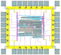
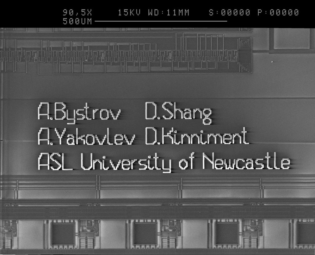
HADIC Chip contains a range of arbiters (three-way and eight-way ordered arbiters, an eight-way static and dynamic priority arbiters, a comparator with a latch for an A/D converter, Asynchronous Communication Mechanism (3-slot Pool).
Year: 2000
Technology: CMOS 0.6um fabricated via Europractice.
Projects: HADES, COMFORT (funded by EPSRC)
Relevant papers:
A. Bystrov, D.J. Kinniment, A. Yakovlev. "Priority Arbiters", Proc. Sixth Int. Symp. on Advanced Research in Asynchronous Circuits and Systems (Async'2000), April 2000, Eilat, Israel, IEEE Computer Society Press, pp. 128-137.
F. Xia, A. Yakovlev, D. Shang, A. Bystrov, A. Koelmans, D.J. Kinniment. "Asynchronous Communication Mechanisms Using Self-timed Circuits", Proc. Sixth Int. Symp. on Advanced Research in Asynchronous Circuits and Systems (Async'2000), April 2000, Eilat, Israel, IEEE Computer Society Press, pp. 150-159.
D. Shang, F. Xia, A. Yakovlev. "Testing a self-timed asynchronous communication mechanism (ACM) VLSI chip", IEEE Workshop on Design and Diagnostics of Electronic Circuits and Systems (DDECS) 2001, Gyor, Hungary, 18-20 April 2001. pp. 53-56.

ASIC for Brushless DC drive controller.
Year: 1993
Technology: CMOS gate array 1um with 20,000 gates used.
The architecture is described in:
"An Integrated Circuit Controller for Brushless D.C. Drives" D.J. Kinniment, P.P. Acarnley, A.G. Jack. EPE Conference, Florence, 3-6 September 1991


Last modified 14/11/2019 by IGC