Tutorials
Tutorial 1 - Monday 7th April 2008, 09:00-10:30 & 11:00-12:00
"Metastability and Synchronisation in SOCs and NOCs", parts 1 & 2. Slides (1.3MB PDF)
David Kinniment, Newcastle University.
Abstract
Synchronization and arbitration is necessary for data communication in networks on chip. Independently clocked synchronous processors in a globally asynchronous system require the data to be synchronized, and arbitration is necessary at routing nodes in the network.
The synchronizer and arbiter circuits that are used to retime and route the data can be subject to metastability, in which the response time can be unbounded, leading to either unreliability or a probability of long response times, as well as high latency in the communication path.
The circuits themselves are not the same as standard gates, as they operate partly in the analog domain, their delays are determined by different parameters, and they can be more sensitive to nanometer scaling effects.
The tutorial will describe metastability, concentrating on the characterization of synchronizers and arbiters, showing how reliable circuits can be designed, how high throughput and low latency systems can be built, and how their actual performance can be measured.
Two demonstrations are scheduled, one in which an asynchronous input is synchronized on an FPGA using different gate configurations to demonstrate the effects of metastability and illustrate how reliability can be predicted from simple measurements. The other will show that prediction is not necessarily straightforward, and very long metastable responses may need to be measured to be sure of the reliability in a high performance system with many components that can become metastable.
Biography
David Kinniment received the MSc in Electrical Engineering (1963) and PhD in Computer Science (1968) from Manchester University, UK, where he was part of the teams involved in the design of the asynchronous ATLAS and MU5 computers. Between 1964 and 1979 he was Assistant Lecturer, Lecturer and Senior Lecturer in the Computer Science Dept at Manchester. In 1979 he was appointed to the Chair of Electronics at Newcastle University, UK, and was Head of the Electrical and Electronic Engineering Dept from 1982-1990, and 1996-1998. He is currently an Emeritus Professor in the University. He works with both the microelectronics group in the Electrical Engineering Dept, and the VLSI group in the Computer Science Dept at Newcastle University where his interests include i.c. design, synchronization, arbitration, and asynchronous systems.
He is the author of around 100 papers, and has recently published a book on "Synchronization and Arbitration in Digital Systems".
Tutorial 2 - Monday 7th April 2008, 13:30-15:30
"Analysis and Optimization of Global Interconnects". Slides (506KB PDF)
Sachin S. Sapatnekar, University of Minnesota.
Abstract
In classical technologies, the delays of a circuit were ``in the gates,'' but today, interconnects are widely acknowledged to constitute the major performance bottleneck. This shift, which is a direct consequence of technology scaling, began to be visible about a decade ago, was slowed down by the move from aluminum to copper interconnects before it accelerated again, and continues to the present day and beyond. In high-performance chips in current and future technologies, the optimization of global wires and busses is critical to meeting system-level constraints.
The talk begins by examining techniques for estimating the delays of on-chip interconnects, capturing a variety of physical effects that affect these wires. The presence of RLC parasitics on a chip contribute to the delay of a wire, and various metrics and performance evaluation techniques may be used. The first part of the talk will provide an overview of delay calculation methods will be provided, with examples, and the accuracy of various commonly-used metrics.
Next, we consider the problem of optimizing global interconnects. For a single net, this can be achieved through techniques such as topology selection and buffering. In realistic designs, a large number of nets contend for a limited set of resources. This competition gets particularly acute with technology scaling, as large numbers of global nets compete to use a limited set of global wiring and buffer resources. The second part of the talk will outline methods for optimizing the topology and design of on-chip interconnects, under these constraints. Finally, we will discuss the implications of these shifts on designs in future technologies.
Biography
Sachin Sapatnekar is the Henle Professor of ECE at the University of Minnesota. He received the PhD degree from the University of Illinois at Urbana-Champaign in 1992, and subsequently taught at Iowa State University before moving to Minnesota in 1997. His research interests are in the areas of optimization problems related to physical design, timing and synthesis, and he has published widely in these areas. He has received several best paper awards and the Semiconductor Research Corporation's Technical Excellence award, and is a fellow of the IEEE.
Tutorial 3 - Monday 7th April 2008, 16:00-17:30
"Synchronous Elastic Systems". Slides (4MB PDF)
Mike Kishinevsky, Intel Corporation.
Abstract
Synchronous elastic (or latency insensitive) systems have been suggested by a few research groups as a form of a discretized asynchronous systems. Such systems are 'time elastic' in a sense that they can tolerate dynamic and static changes in latencies of computation and communication components. Therefore, they enable new micro-architectural trade-offs, e.g. a wider use of variable latency components targeting average case optimization, rather than the worst case optimization traditional to regular synchronous circuits. They also enable correct-by-construction re-pipelining of wires and computation blocks - a useful feature that can simplify design and RC scaling in the nano-scale technologies. In comparison with continuous time asynchronous systems (operating without a clock) synchronous elastic have a few advantages: complete reuse of the synchronous CAD tools and design practices and negligible overhead in area and delay (if constructed using an efficient technique).
We first review design of synchronous elastic using lazy evaluation: the block is initiated only when all input tokens of information got arrived. We then present an optimized implementation relying on early evaluation that aims at speeding-up computations by enabling computational nodes as soon as the needed input values are available.
We will review how elastic systems are modeled with Marked Graphs and their extensions (to cover early evaluation behavior), describe performance analysis and optimization methods and review applications, including application to transport layer of an NoC design.
Biography
Mike Kishinevsky leads a research group in front-end design at Strategic CAD Labs of Intel Corporation. He received his PhD degree in CS from the Electro-technical University of St.Petersburg, Russia. Prior to joining Intel in 1998 Mike has been a Research Fellow at Russian Academy of Science, a Senior Researcher at R&D Coop TRASSA (a start-up in asynchronous design), a visiting Associate Professor at the Technical University of Denmark, and a Professor at the University of Aizu, Japan. He co-authored three books in asynchronous design and has published over 70 journal and conference papers. Mike has served on the technical program committee at several conferences and workshops.
Keynote Talks
Keynote Talk Async-1 - Tuesday 8th April 2008, 08:30-09:30 - Chair: Jordi Cortadella
"Asynchronous circuit technology is on the market". Slides (1.5MB PDF)
Ad Peeters & Arjan Bink, Handshake Solutions.
Abstract
The seventh international symposium on asynchronous circuits and systems, in Salt Lake City, March 2001, featured a presentation with the challenging title 'Where are the Async Millionaires?'
The morale of this invited talk by Kevin Normoyle, a Distinguished Engineer at Sun Microsystems, was that if the asynchronous community claims that their technology is so promising, why doesn't the technology create Greed and Fear. Greed in the sense that asynchronous technology might enable you to outperform your competition by exploiting unique possibilities, and Fear that the competition may be doing this. The talk demonstrated an absence of Fear and Greed in the area of high performance computing. The number of asynchronous millionaires was proposed as a way to measure success.
We are now at the fourteenth ASYNC conference in Newcastle, and seven years have passed. Today, hundreds of millions of asynchronous circuits are produced every year, and many of us may use it on a daily basis without being aware of it. As an example, asynchronous circuits designed using Handshake Solutions' Timeless Design Environment (TiDE) may be found in the vast majority of electronic (biometric) passports, in in-vehicle networks like CAN and LIN, in MEMS-based sensors such as for measuring tire pressure, in access-control systems, and in Near Field Communication devices such as Nokia's 6131 NFC phone.
In the talk I would want to address some of the steps that have been taken to bring this disruptive technology to the market, and the challenges that had and have to be overcome. It is now obvious to me that asynchronous technology can create Greed and Fear. It should be only a matter of time before the first asynchronous millionaires arise.
Biographies
Ad Peeters is the CTO of Handshake Solutions, a business created by Royal Philips Electronics to bring asynchronous technology to the market. Ad has pushed Handshake Technology since his MSc and PhD work at Eindhoven University and Philips Research, and will continue to drive the growth of Handshake Solutions until he is a millionaire.
Arjan Bink is the Chief Design Engineer of Handshake Solutions. He graduated of the Technical University of Eindhoven, having studied Computer Science and Technological Design. It was during this time that he was involved in the work on the Single Track handshake protocol at Philips Research.
In 1995, Arjan joined Philips Research where he was involved in numerous processor-related projects looking at power reduction, clockless design, processor architectures (microprocessors, digital signal processors and multi-processor configurations). He then spent two years in the Strategic ASIC Group at Philips Semiconductors working on advanced prototyping architectures and System-on-Chip (SoC) design.
Arjan joined Handshake Solutions in 2003 and is responsible for self-timed processor design, e.g. the ARM996HS.
Keynote Talk NoCS-1 - Wednesday 9th April 2008, 08:30-09:30 - Chair: Simon Moore
"Past, present and future communicating processors". Slides (73KB PDF)
David May, Department of Computer Science, University of Bristol, UK.
Abstract
Multiprocessor chips are here - and over the next decade they will scale to hundreds of communicating processors per chip. They offer the possibility of computer systems scaling to millions of processors. But perhaps more important is that they will make it possible to design electronic systems using concurrent software to program high-volume multiprocessor chips. Individual processors in these systems will be used to execute conventional software, or to emulate functions normally performed by hardware. And communicating processors - programmed in terms of communicating processes - provide a natural way to unify approaches to hardware and software design.
Biography
David May is Professor and Head of Computer Science at Bristol University. Before joining the university in 1995, he worked for 16 years in the microelecronics industry, joining Inmos (now STMicroelectronics) at its formation in 1979. He is well known for his work on innovative microprocessors including the Inmos transputer. He is the author of over 100 papers and patents, and has given numerous conference presentations.
In 1990 he was elected a Fellow of the Royal Society for his contributions to computer architecture and parallel computing. David's current research interests are in microprocessor architecture; system design and verification; mobile, wearable and pervasive computing. He maintains active relationships with industry and technology investors, and is on the Technical Advisory Boards of several recent microelectronics design companies. Alongside this, he has advised on intellectual property issues and acted as an expert witness in litigation.
His most recent interests are as CTO of XMOS (microcomputers), director of Mista (location-based services), and co-founder of the Bristol Robotics Labs (fun!).
Keynote Talk Async-2 - Thursday 10th April 2008, 08:30-09:30 - Chair: Erik Brunvand
"Statistical device variability and its impact on design". Slides (2.9MB PDF)
Asen Asenov, Device Modeling Group, Department of Electronics and Electrical Engineering, University of Glasgow, UK.
Abstract
It is widely recognised that the uncontrollable statistical variability in device characteristics represent major challenges to scaling and integration for present and next generation nano-CMOS transistors and circuits. This will in turn demands revolutionary changes in the way in which future integrated circuits and systems are designed. Strong links must be established between circuit design, system design and fundamental device technology to allow circuits and systems to accommodate the increasing statistical variability. This will add significant complexity to the design process, requiring orchestration of a broad spectrum of design tools by geographically distributed teams of device experts, circuit and system designers.
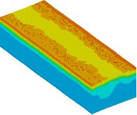
Fig. 1 Random discrete dopants in combination with line edge roughness in a 35 nm MOSFET from the present 90 nm technology node.
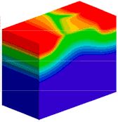
Fig. 2 Impact of the poly-Si gate granularity on the potential distribution in a 30 nm MOSFET.
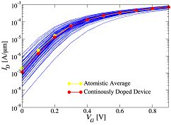
Fig. 3 Random dopant induced variations in the current-voltage characteristics of 200 transistors with different dopant distributions.
In this talk we review the major sources of variability in CMOS devices focusing at and beyond 45nm technology generation and beyond. The focus is on intrinsic parameter fluctuations introduced by discreteness of charge and matter, which play an increasingly important role in the present and future CMOS devices and cannot be controlled or reduced by tightening the process tolerances. One of the most important sources of intrinsic parameter fluctuations illustrated in are the random discrete dopants in combination with line edge roughness (Fig. 1) and the poly silicon gate granularity (Fig. 2) which makes every transistor microscopically different from its counterparts and introduces differences in the characteristics of topologically identical devices (Fig. 3). The corresponding parameter variations already affect adversely the yield and the functionality and limit the scalability of SRAM cells. We will present results forecasting the magnitude of the statistical device variability in the next technology generations based on comprehensive physical 3D statistical simulation. A methodology for transferring of this information into industry standard compact models like BOSIM4 and BISIMSOI will also be presented. The use of compact models in statistical circuit simulations will be illustrated in the case of SRAM design.
Biography
Asen Asenov received his MSc degree in solid state physics from Sofia University, Bulgaria in 1979 and the PhD degree in physics from The Bulgarian Academy of Science in 1989.
He is a professor of Device Modelling, Leader of the Glasgow Device Modelling Group and Academic Director of the Glasgow Process and Device Simulation Centre he coordinates the development of 2D and 3D quantum mechanical, Monte Carlo and classical device simulators and their application in the design of advanced and novel CMOS devices. He has pioneered the simulations of statistical variability in nano-CMOS devices including random dopants, interface roughness and line edge roughness. He has over 400 publications in the above areas.
Keynote Talk NoCS-2 - Friday 11th April 2008, 08:30-09:30 - Chair: Pascal Vivet
"Optical Interconnects for Backplane and Chip-to-chip Photonics". Slides (4.6MB PDF)
Ian H. White and Richard V. Penty, Electrical Engineering Division, Engineering Department, University of Cambridge, UK.
Abstract
The growth in computing power has placed increasing demands on low cost technologies for the transmission of large bandwidths over short distances using highly compact forms. As a result, in recent years a diverse range of photonic technologies have been developed not only to allow high speed point-to-point links, but also to enable the simple creation of networks within computing infrastructure, and indeed to allow an element of reconfiguration. In addition, related work has sought to make possible such functions directly on chip using new silicon based technologies.
Following a general review of the field, this paper will illustrate new cost effective optical technologies, developed at Dow Corning, which can be formed directly on printed circuit boards using materials that withstand solder overflow. The technology has the potential of delivering both board-to-board and chip-to-chip communications. For typical required lengths, polymer waveguides can be formed which are essentially bit rate transparent with high crosstalk performance. With readily available parallel optics, this allows a high capacity (of Terabit order) backplane performance. Recent results show efficient high-speed data transmission at 10 Gbps individual channel rates with low loss and excellent crosstalk performance.
The paper will conclude by reporting how we are exploring the potential extension of this technology for use in high-speed on-board optical networks.
Biography
Prof. Ian White is currently van Eck Professor of Engineering, Chair of the Council, School of Technology and Head of the Photonic Research Group in the Engineering Department at the University of Cambridge. He gained his B.A. and Ph.D. degrees from the University of Cambridge, England, in 1980 and 1984. He then was appointed a research fellow and assistant lecturer at the University of Cambridge before moving to become Professor of Physics at the University of Bath in 1990. In 1996 he moved to the University of Bristol, becoming Head of the Department of Electrical and Electronic Engineering in 1998, before returning to the University of Cambridge in October 2001.
Ian White has built up a substantial research activity in the field of optoelectronics and optical communications and his team numbers approximately 40 people publishing on average 60 papers a year. Highlights of Ian’s research have included: the first negative chirp electro-absorption modulator and the invention of a technique for transmitting radio frequency signals over long distances of multimode optical fibre. Several of these advances have already made commercial impact, the offset launch technique for enhancing the bandwidth of optical fibre links having been adopted within Gigabit Ethernet standard, and a technique for the polarization pinning of VCSELs having been employed in laser optical mice. He has chaired the channel model sub-task force of the IEEE 10 GbE LRM standard. The Institution of Electrical Engineers has awarded him the Blumlein-Browne-Willans Prize and the Ambrose Fleming Premium Award. Ian is currently an editor-in-chief of Electronics Letters and is also a co-founder of ZinWave.
